- 您现在的位置:买卖IC网 > Sheet目录1997 > ICS813076CYILF (IDT, Integrated Device Technology Inc)IC VCXO-PLL WIRELESS 64-TQFP
FREQUENCY GENERATOR/JITTER ATTENUATION DEVICE
FOR WIRELESS INFRASTRUCTURE APPLICATIONS
ICS813076I
IDT / ICS FREQUENCY GENERATOR/JITTER ATTENUATION
1
ICS813076CYI REV. A JULY 8, 2008
GENERAL DESCRIPTION
The ICS813076I is a member of the HiperClocks
family of high performance clock solutions from IDT.
The ICS813076I a PLL based synchronous clock
solution that is optimized for wireless infrastructure
equipment where frequency translation and jitter
attenuation is needed.
The device contains two internal PLL stages that are cascaded
in series. The first PLL stage attenuates the reference clock jitter
by using an internal or external VCXO circuit. The internal VCXO
requires the connection of an external inexpensive pullable
crystal (XTAL) to the ICS813076I. This first PLL stage (VCXO
PLL) uses external passive loop filter components which are used
to optimize the PLL loop bandwidth and damping characteristics
for the given application. The output of the first stage VCXO PLL
is a stable and jitter-tolerant reference input for the second PLL
stage of 30.72MHz. The second PLL stage provides frequency
translation by multiplying the output of the first stage up to
614.4MHz. The low phase noise characteristics of the clock
signal is maintained by the internal FemtoClock PLL, which
requires no exter nal components or configuration. Two
independently configurable frequency dividers translate the
491.52MHz or 614.4MHz internal VCO signal to the desired output
frequencies. All frequency translation ratios are set by device
configuration pins. Alternative to the clock frequency multiplication
functionality, the ICS813076I can work as a VCXO. Enabling the
VCXO mode allows the output frequency of 614.4MHz/N or
491.52MHz/N to be pulled by the input voltage of the VC pin.
Supported input reference clock frequencies:
15.36MHz,
30.72MHz
61.44MHz
Supported output clock frequencies:
30.72MHz
122.88MHz
153.6MHz
491.52MHz
614.4MHz
FEATURES
Two operation modes: input frequency multiplier and VCXO
Nine differential LVPECL outputs, organized in three indepen-
dent output banks
Two selectable differential input clocks can accept the following
differential input levels: LVDS, LVPECL, LVHSTL, SSTL, HCSL
Maximum output frequency: 614.4MHz
FemtoClock VCO frequency: 491.52MHz or 614.4MHz (typical)
Frequency generation optimized for wireless infrastructure
equipment
Attenuates the phase jitter of the input clock signal by using a
low-cost pullable fundamental mode crystal (XTAL)
Multiplies the input clock frequency by 1, 4, 5, 16 or 20
LVCMOS/LVTTL levels for all input/output controls
PLL fast-lock control
VCXO PLL bandwidth can be optimized for jitter attenuation
and reference frequency tracking using external loop filter
components
Absolute pull range: ±50ppm
RMS phase jitter (12kHz – 20MHz): 0.97ps (typical)
Full 3.3V supply
-40°C to 85°C ambient operating temperature
Available in lead-free (RoHS 6) package
For other devices supporting wireless infrastructure clock
frequencies, please refer to ICS813076I-02, ICS813076I-30,
ICS813076I-31 and ICS814075I
HiPerClockS
ICS
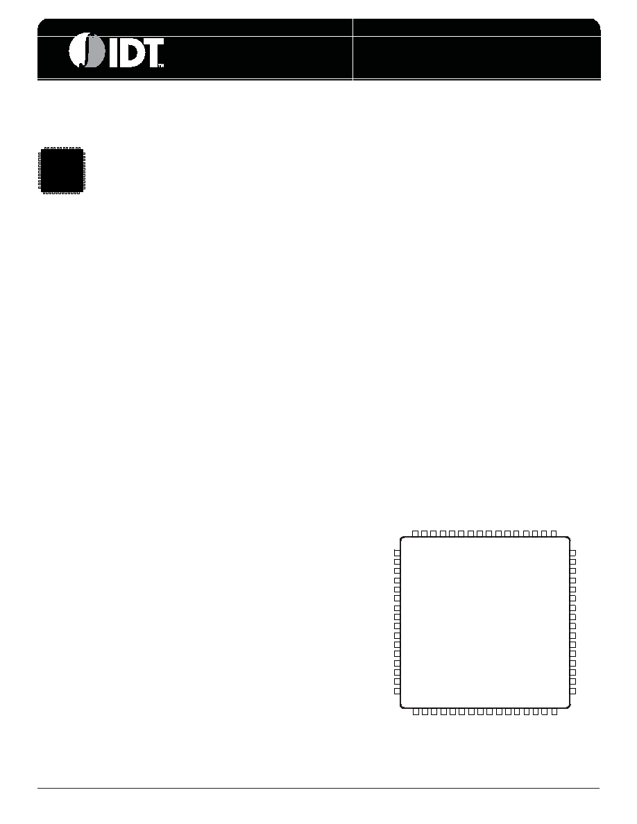
PIN ASSIGNMENT
1
2
3
4
5
6
7
8
9
10
11
12
13
14
15
16
LF1
LF0
ISET
VC
FLM
VCC
CLK1
nCLK1
nMR
CLK0
nCLK0
VEE
LOCK
VCCO
NA_SEL1
nQA1
QA1
VCCO
nQA2
QA2
VEE
nQA3
QA3
VCCO
nQA4
QA4
VCC
VEE
nQB0
QB0
VCCO
ICS813076I
64-Lead TQFP, E-Pad
10mm x 10mm x 1.0mm
package body
Y package
Top View
48
47
46
45
44
43
42
41
40
39
38
37
36
35
34
33
64 63 62 6160 59 58 57 56 55 5453 52 51 50 49
nQA0
QA0
V
CCO
nQC
QC
V
CCO
V
EE
nc
MF_SEL
MV_SEL
VC_SEL
V
CC
XT
AL_OUT
XT
AL_IN
V
EE
nQB1
QB1
V
CCO
nQB2
QB2
V
CCA
nc
REF_SEL
nST
OP
nBYP
A
S
P
NC_SEL0
NC_SEL1
NB_SEL0
NB_SEL1
NA_SEL0
1718 19 20 21 22 23 24 25 26 27 28 29 30 31 32
发布紧急采购,3分钟左右您将得到回复。
相关PDF资料
ICS813078BYILF
IC VCXO PLL WIRELESS 64TQFP
ICS813323BGLF
IC ATTENUATOR/MULTIPLIER 24TSSOP
ICS840002AGLF
IC FREQ SYNTHESIZER 16-TSSOP
ICS840022AKI-02LF
IC CLOCK GENERATOR 16VFQFPN
ICS84021AYLF
IC SYNTHESIZER HIGH FREQ 32-LQFP
ICS840245AGILF
IC FREQ SYNTHESIZER 16-TSSOP
ICS8402AYILF
IC FREQ SYNTHESIZER 32-LQFP
ICS841602AGILF
IC CLOCK GENERATOR 28-TSSOP
相关代理商/技术参数
ICS813076CYILFT
功能描述:IC VCXO-PLL WIRELESS 64-TQFP RoHS:是 类别:集成电路 (IC) >> 时钟/计时 - 专用 系列:HiPerClockS™, FemtoClock™ 标准包装:1,500 系列:- 类型:时钟缓冲器/驱动器 PLL:是 主要目的:- 输入:- 输出:- 电路数:- 比率 - 输入:输出:- 差分 - 输入:输出:- 频率 - 最大:- 电源电压:3.3V 工作温度:0°C ~ 70°C 安装类型:表面贴装 封装/外壳:28-SSOP(0.209",5.30mm 宽) 供应商设备封装:28-SSOP 包装:带卷 (TR) 其它名称:93786AFT
ICS813078BYILF
功能描述:IC VCXO PLL WIRELESS 64TQFP RoHS:是 类别:集成电路 (IC) >> 时钟/计时 - 专用 系列:HiPerClockS™, FemtoClock™ 标准包装:1,500 系列:- 类型:时钟缓冲器/驱动器 PLL:是 主要目的:- 输入:- 输出:- 电路数:- 比率 - 输入:输出:- 差分 - 输入:输出:- 频率 - 最大:- 电源电压:3.3V 工作温度:0°C ~ 70°C 安装类型:表面贴装 封装/外壳:28-SSOP(0.209",5.30mm 宽) 供应商设备封装:28-SSOP 包装:带卷 (TR) 其它名称:93786AFT
ICS813078BYILFT
功能描述:IC VCXO PLL WIRELESS 64TQFP RoHS:是 类别:集成电路 (IC) >> 时钟/计时 - 专用 系列:HiPerClockS™, FemtoClock™ 标准包装:1,500 系列:- 类型:时钟缓冲器/驱动器 PLL:是 主要目的:- 输入:- 输出:- 电路数:- 比率 - 输入:输出:- 差分 - 输入:输出:- 频率 - 最大:- 电源电压:3.3V 工作温度:0°C ~ 70°C 安装类型:表面贴装 封装/外壳:28-SSOP(0.209",5.30mm 宽) 供应商设备封装:28-SSOP 包装:带卷 (TR) 其它名称:93786AFT
ICS813078I
制造商:IDT 制造商全称:Integrated Device Technology 功能描述:FEMTOCLOCKS? VCXO-PLL FREQUENCY GENERATOR FOR WIRELESS INFRASTRUCTURE EQUIPMENT
ICS813252CKI-02LF
功能描述:IC MULTIPLIER VCXO PLL 32-VFQFPN RoHS:是 类别:集成电路 (IC) >> 时钟/计时 - 时钟发生器,PLL,频率合成器 系列:HiPerClockS™, FemtoClock™ 标准包装:27 系列:Precision Edge® 类型:频率合成器 PLL:是 输入:PECL,晶体 输出:PECL 电路数:1 比率 - 输入:输出:1:1 差分 - 输入:输出:无/是 频率 - 最大:800MHz 除法器/乘法器:是/无 电源电压:3.135 V ~ 5.25 V 工作温度:0°C ~ 85°C 安装类型:表面贴装 封装/外壳:28-SOIC(0.295",7.50mm 宽) 供应商设备封装:28-SOIC 包装:管件
ICS813252CKI-02LFT
功能描述:IC MULTIPLIER VCXO PLL 32-VFQFPN RoHS:是 类别:集成电路 (IC) >> 时钟/计时 - 时钟发生器,PLL,频率合成器 系列:HiPerClockS™, FemtoClock™ 标准包装:27 系列:Precision Edge® 类型:频率合成器 PLL:是 输入:PECL,晶体 输出:PECL 电路数:1 比率 - 输入:输出:1:1 差分 - 输入:输出:无/是 频率 - 最大:800MHz 除法器/乘法器:是/无 电源电压:3.135 V ~ 5.25 V 工作温度:0°C ~ 85°C 安装类型:表面贴装 封装/外壳:28-SOIC(0.295",7.50mm 宽) 供应商设备封装:28-SOIC 包装:管件
ICS813252I-02
制造商:IDT 制造商全称:Integrated Device Technology 功能描述:VCXO JITTER ATTENUATOR & FEMTOCLOCK? MULTIPLIER
ICS813253BGLF
功能描述:IC ATTENUATOR/XLATOR 24TSSOP RoHS:是 类别:集成电路 (IC) >> 时钟/计时 - 时钟发生器,PLL,频率合成器 系列:HiPerClockS™, FemtoClock™ 标准包装:27 系列:Precision Edge® 类型:频率合成器 PLL:是 输入:PECL,晶体 输出:PECL 电路数:1 比率 - 输入:输出:1:1 差分 - 输入:输出:无/是 频率 - 最大:800MHz 除法器/乘法器:是/无 电源电压:3.135 V ~ 5.25 V 工作温度:0°C ~ 85°C 安装类型:表面贴装 封装/外壳:28-SOIC(0.295",7.50mm 宽) 供应商设备封装:28-SOIC 包装:管件